我们的优势
1.技术保障:国内顶尖技术博士团队,从事相关工作5年以上,发表众多高水平论文。
2.制备条件:完善先进的实验设备(迈塔光电精密定点转移平台、奥林巴斯金相显微镜、威格手套箱),齐全的二维材料(特殊材料除外),客户仅需提供器件结构图即可。
3.制备周期:材料剥离表征转移到器件完成整个工序,根据二维材料剥离难易程度货期会略有不同。正常货期约为1~2周。
4.材料表面洁净度:材料表面为原子级洁净。
5.可定制不同材料不同材质不同层数的异质结
一、可定制3种二维材料异质结:
(1)二维/二维异质结:不同种类二维材料形成的异质结。
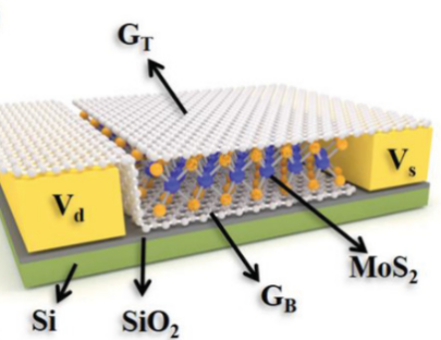
Gao S, Wang Z, Wang H, et al. Graphene/MoS2/Graphene Vertical Heterostructure‐Based Broadband Photodetector with High Performance [J]. Advanced Materials Interfaces, 2021, 8(3): 2001730.
(2)零维/二维异质结:零维材料(量子点)与二维材料形成的异质结。
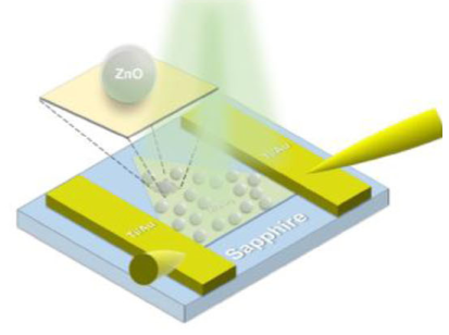
Zhou Y H, Zhang Z B, Xu P, et al. UV-visible photodetector based on I-type heterostructure of ZnO-QDs/monolayer MoS2 [J]. Nanoscale research letters, 2019, 14(1): 1-10.
(3)零维/一维异质结:一维材料(纳米线)与二维材料形成的异质结。
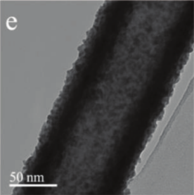
Zhang Y, Zhang F, Wu L, et al. Van der Waals Integration of Bismuth Quantum Dots–Decorated Tellurium Nanotubes (Te@ Bi) Heterojunctions and Plasma‐Enhanced Optoelectronic Applications[J]. Small, 2019, 15(47): 1903233.
二、制备方法:
(1)二维/二维异质结:干转移法等。下图为干转移法制备三种二维材料组成的异质结的过程示意图。
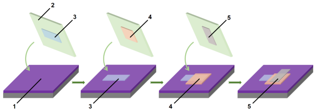
(2)零维/二维异质结:旋涂法、浸泡法等。下图为旋涂法制备一维/二维异质结的过程示意图。

(3)零维/一维异质结:化学法等。下图为化学法制备零维Bi/一维Te异质结的结果表征,结果表明异质结构中零维Bi几乎均匀地分布在一维Te纳米管的表面。
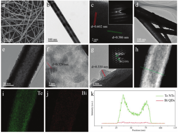
Zhang Y, Zhang F, Wu L, et al. Van der Waals Integration of Bismuth Quantum Dots–Decorated Tellurium Nanotubes (Te@ Bi) Heterojunctions and Plasma‐Enhanced Optoelectronic Applications[J]. Small, 2019, 15(47): 1903233.
三、应用领域:
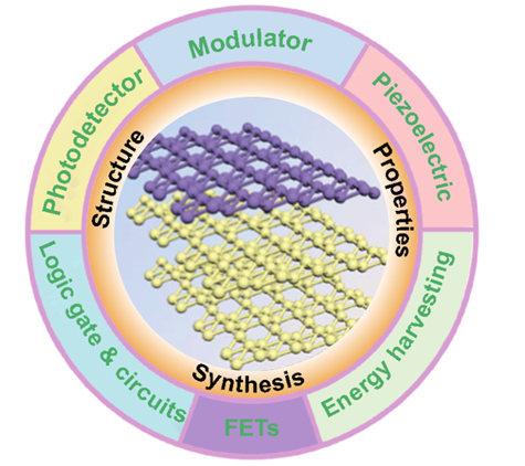
如下图所示,异质结在很多领域具有广泛应用。例如电子器件、光电器件、压电器件、能源应用等。
四、 所发表的相关论文
Construction of multiple interfaces and dielectric/magnetic heterostructures in electromagnetic wave absorbers with enhanced absorption performance: A review | JOURNAL OF MATERIOMICS |
| A Regioselectively Oxidized 2D Bi/BiOx Lateral Nano-Heterostructure for Hypoxic Photodynamic Therapy | ADVANCED MATERIALS |
Repression of Interlayer Recombination by Graphene Generates a Sensitive Nanostructured 2D vdW Heterostructure Based Photodetector | ADVANCED SCIENCE |
Designing of 0D/2D mixed-dimensional van der waals heterojunction over ultrathin g-C3N4 for high-performance flexible self-powered photodetector | CHEMICAL ENGINEERING JOURNAL |
Recent progress and strategies in photodetectors based on 2D inorganic/organic heterostructures | 2D MATERIALS |
Graphene/MoS2/Graphene Vertical Heterostructure-Based Broadband Photodetector with High Performance | ADVANCED MATERIALS INTERFACES |
Electronic structure engineering on two-dimensional (2D) electrocatalytic materials for oxygen reduction, oxygen evolution, and hydrogen evolution reactions | NANO ENERGY |
2D van der Waals heterostructures: processing, optical properties and applications in ultrafast photonics | MATERIALS HORIZONS |
Zero-Dimensional MXene-Based Optical Devices for Ultrafast and Ultranarrow Photonics Applications | ADVANCED SCIENCE |
Transport and Thermoelectric Properties of SnX (X = S or Se) Bilayers and Heterostructures | ACS APPLIED ENERGY MATERIALS |
Recent Advances in Twisted Structures of Flatland Materials and Crafting Moire Superlattices | ADVANCED FUNCTIONAL MATERIALS |
Review of 2D group VA material-based heterostructures | JOURNAL OF PHYSICS D-APPLIED PHYSICS |
Manipulating Charge and Energy Transfer between 2D Atomic Layers via Heterostructure Engineering | NANO LETTERS |
Black phosphorus-based van der Waals heterostructures for mid-infrared light-emission applications | LIGHT-SCIENCE & APPLICATIONS |
Photoluminescence enhancement of MoS2/CdSe quantum rod heterostructures induced by energy transfer and exciton-exciton annihilation suppression | NANOSCALE HORIZONS |
Multifunctional VI-VI binary heterostructure-based self-powered pH-sensitive photo-detector | JOURNAL OF MATERIALS CHEMISTRY C |
Site-Selective Bi2Te3-FeTe2 Heterostructure as a Broadband Saturable Absorber for Ultrafast Photonics | LASER & PHOTONICS REVIEWS |
Recent advances in black phosphorus/carbon hybrid composites: from improved stability to applications | JOURNAL OF MATERIALS CHEMISTRY A |
Recent developments in emerging two-dimensional materials and their applications | JOURNAL OF MATERIALS CHEMISTRY C |
Highly Efficient Silicon Photonic Microheater Based on Black Arsenic-Phosphorus | ADVANCED OPTICAL MATERIALS |
UV-Visible Photodetector Based on I-type Heterostructure of ZnO-QDs/Monolayer MoS2 | NANOSCALE RESEARCH LETTERS |
Fully photon modulated heterostructure for neuromorphic computing | NANO ENERGY |
In situ preparation of a CsPbBr3/black phosphorus heterostructure with an optimized interface and photodetector application | NANOSCALE |
Van der Waals heterostructures for optoelectronics: Progress and prospects | APPLIED MATERIALS TODAY |
Graphene Heterostructure Integrated Optical Fiber Bragg Grating for Light Motion Tracking and Ultrabroadband Photodetection from 400 nm to 10.768 mu m | ADVANCED FUNCTIONAL MATERIALS |
Highly Efficient and Air-Stable Infrared Photodetector Based on 2D Layered Graphene-Black Phosphorus Heterostructure | ACS APPLIED MATERIALS & INTERFACES |
Synthesis of Ultrathin Composition Graded Doped Lateral WSe2/WS2 Heterostructures | ACS APPLIED MATERIALS & INTERFACES |
Tuning of Interlayer Coupling in Large-Area Graphene/WSe2 van der Waals Heterostructure via Ion Irradiation: Optical Evidences and Photonic Applications | ACS PHOTONICS |
A black/red phosphorus hybrid as an electrode material for high-performance Li-ion batteries and supercapacitors | JOURNAL OF MATERIALS CHEMISTRY A |
Graphene-Bi2Te3 Heterostructure as Broadband Saturable Absorber for Ultra-Short Pulse Generation in Er-Doped and Yb-Doped Fiber Lasers | IEEE JOURNAL OF SELECTED TOPICS IN QUANTUM ELECTRONICS |
On-Nanowire Axial Heterojunction Design for High-Performance Photodetectors | ACS NANO |
Harmonic mode-locking and wavelength-tunable Q-switching operation in the graphene-Bi2Te3 heterostructure saturable absorber-based fiber laser | OPTICAL ENGINEERING |
Photoelectrochemical-type sunlight photodetector based on MoS2/graphene heterostructure | 2D MATERIALS |
Graphene-Bi2Te3 Heterostructure as Saturable Absorber for Short Pulse Generation | ACS PHOTONICS |